Privacy statement: Your privacy is very important to Us. Our company promises not to disclose your personal information to any external company with out your explicit permission.
Select Language
The IC open-short test is divided into open short to VDD and open short to VSS.
In general, each pin of the chip has a bleeder or protection circuit. Two diodes are connected end to end. One end is connected to VDD, and the other end to VSS. The signal is coming from the junction of two diodes. When testing, first test the chip. The VDD pin is connected to 0 volts (or ground), and each chip pin is supplied with a current of 100uA to 500uA from the tester to the chip. The current flows through the upper diode to VDD (0V), and then the voltage of the pin is measured. The normal value should be a diode deviation voltage of about 0.7 volts. We generally set the upper limit to 1.5 volts, the lower limit to 0.2 volts, to more than 1.5 volts to determine openfail, and to less than 0.2 volts to determine shortfail. This is the open_short_to_VDD test.
The principle of the open_short_to_VSS test is basically the same. Similarly, VDD is first connected to 0 volts, and then a chip is provided to test the current. The current flows from VSS to the tester through the lower diode. Then measure the pin voltage, the same normal value should be a diode deviation voltage of about 0.7 volts, but the voltage is in the opposite direction, the upper limit is still 1.5 volts, the lower limit is 0.2 volts, greater than 1.5 volts is judged as openfail, less than 0.2 volts is judged as Shortfail. This is the open_short_to_VSS test.
Overall design
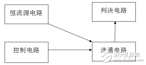
(a) hardware design
1. Constant current circuit design

The 5V voltage source generates 2.5V through the circuit for use by the current source. The current source is formed by connecting the bases of Q1 and Q2 PNP transistors together with three resistors as shown in the upper right figure. The current source is mainly used to provide 100mA to 500mA of current for testing the input, in which the C4 capacitor is mainly Power off in an instant and act as a buffer
2. Decision circuit design

The comparison circuit is terminated with 2.5V, and a voltage of 1.5V is generated on the 2nd pin of the chip LM358AM through the voltage division of the resistor, and a voltage of 0.2V is generated on the 5th pin; the pinpots of the 3rd and 6th pins are compared with their potentials. In this way, the diode D1 or D2 is gated. When the potentials of pins 3 and 6 are higher than 1.5V or lower than 0.2V, one of the diodes is turned on. When the potential is between two potentials, both diodes are turned off. Pin 6 is equal to the potential of the U3 pin.
3. Control circuit design

The control circuit is mainly realized through the AT89S52 programming control pins U6 and U3 6, 9, 10, 11; the upper right figure is the AT89S52 reset circuit.
4. Strobe circuit design

The gating circuit is mainly used to select the pin of the chip under test. The pin of the U2 gate of the chip is set to 0 through the pin 3 of the chip, and the pin of the chip U3 is placed on the pin of the chip U3. The same level, then through the LED to show whether the two pins are open or short circuit, or normal.
(two) software design#include"reg52.h"
#include"intrins.h"
#define uint unsigned int
#define uchar unsigned char
Sbit P1_0 = P1^0; // defines p1.0
Sbit P1_1 = P1^1; // Define port P1.1
Void deplay(uint z) //Delay
{
Uint x,y;
For(x=z;x"0;x--)
For(y=110;y"0;y--);
}
Void open_short_to_VDD() //Open circuit test
{
Uint i,j;
P2=0x34;
i=P2&0x0f;
j=(P2&0xf0)""4;
For(i=3;i<<=6;i++)
{if(j==i) conTInue;
P2 = (j "4" | i;
If(P1_0)P1_1 =1;else P1_1 =0;
Deplay(700);
}
}
Void open_short_to_VSS() //short circuit test
{
Uint i,j;
P2=0x23;
i=P2&0x0f;
j=(P2&0xf0)""4;
For(i=3;i<<=6;i++)
{
If(i==j) conTInue;
P2 = (j "4" | i;
Deplay(700);
}
}
Void short_out_to_PIN() // Short circuit to each pin
{uint i,j;
P2=0x32;
i=P2&0x0f;
j=(P2&0xf0)""4;
For(i=3;i<<=6;i++)
{
For(j=3;j<<=6;j++)
{
If(j==i) conTInue;
P2 = (j "4" | i;
Deplay(1000);
}
}
}
Main()
{
While(1)
{
open_short_to_VDD();
Deplay(700);
open_short_to_VSS();
Deplay(700);
short_out_to_PIN();
}
}
system designHardware schematic

test

The brightest yellow light in front shows that the chip is OK, and the red light behind indicates the power
E-mel kepada pembekal ini

Privacy statement: Your privacy is very important to Us. Our company promises not to disclose your personal information to any external company with out your explicit permission.

Fill in more information so that we can get in touch with you faster
Privacy statement: Your privacy is very important to Us. Our company promises not to disclose your personal information to any external company with out your explicit permission.