Privacy statement: Your privacy is very important to Us. Our company promises not to disclose your personal information to any external company with out your explicit permission.
Select Language
Application of the new narrowband FM receiver integrated circuit MC3362 / MC3363 / MC3364 / MC3367
The appearance of the MC3362 series of single-chip receiver circuits has greatly promoted the innovation of mobile communication stations. The common characteristics of these integrated circuit chips are: strong function, monolithic, low voltage, low power consumption, and high sensitivity.
The new low-power narrow-band FM monolithic receiver circuit MC3362 already includes a front-end circuit in addition to the high-frequency amplifier, and also adds a carrier detection circuit and a comparator for FSK detection, which is suitable for narrow-band voice and data links Communication. The external lead diagram of MC3362 is shown in Figure 8-1.
The MC3362 contains two local oscillators, two mixing frequencies and two intermediate amplifier circuits. It is a full quadratic superheterodyne receiving circuit from the antenna input to the audio preamplifier output. The first mixing frequency of MC3362 can exceed 450MHz. The first local oscillator can use a flexible LC oscillation circuit, or it can be used as the VCO of the PLL frequency synthesizer. The operating frequency can reach 190MHz. When the RF input is 450MHz, it can also be driven by an external oscillator (100mV).
MC3362 has very good sensitivity and image suppression ability, 12dBSINAD (signal ratio), the sensitivity is 0.7μV. Can be used for FSK data communication. Received signal field strength indicator with 60dB dynamic range. It can be used to control the hand-off and idle communication detection of central and non-central mobile communication devices.
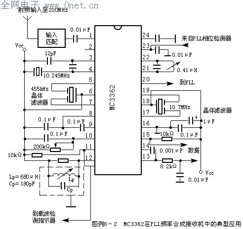
Figure 8-2 shows a typical application example of MC3362. The input RF signal is amplified by the first mixer (18dB), and mixed and converted into a first intermediate frequency signal (10.7MHz). The first intermediate frequency signal is filtered by an external band-pass ceramic filter, and then input to the second mixing frequency The amplifier is further amplified (22dB) and mixed into a second intermediate frequency signal (255kHz). After the second intermediate frequency signal is filtered by an external band-pass ceramic filter, it is input to a limiting amplifier and an electric frequency detection circuit, and finally recovered into an audio signal output through a phase shift discriminator. In addition, the level detection circuit is used to monitor the field strength of the input RF signal, and the data shaping comparison circuit is used to detect the zero-crossing rate of the FSK modulated signal. The rate of data detected by the circuit is 2000-35000 baud.

MC3363 adds a high discharge tube and noise suppression circuit on the basis of MC3362, so the sensitivity is higher and the performance is better. The functional block diagram of MC3363 is shown in Figure 8-3. Due to the addition of a high-level amplifier, the sensitivity of 12dBSINAD can reach 0.3μV.
The chip is particularly suitable for cordless phones.

Fig. 8-4 Typical application example of 4MC3363 synthesizing cordless telephone receiver at PLL frequency. MC3363 and large-scale dual PLL circuit MC14516617 form a 310-channel two-chip frequency synthesis receiver. The first local oscillator of MC3363 is used as the PLL's VCO.
The squelch circuit of this circuit adopts the signal-triggered squelch mode, which controls the squelch muffler switch by the output signal field strength detection circuit output level (13 feet). Similarly, MC3363 can also form a noise-type squelch circuit, as long as the op amp dynamic noise filter, radio frequency NPN tube or data comparator is used as a squelch switch.

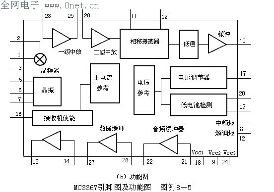
MC3367 is a low-voltage primary superheterodyne receiver circuit. The circuit is simple. Because there is no second mixing and two local oscillators, its harmonic interference is small, and its intermediate frequency gain requirements are also particularly high. Because the MC3367 uses isolation measures, it is not easy to excite itself. MC3367 pin diagram and function diagram are shown in legend 8-5 (a), (b). It includes oscillator, mixer, two-stage intermediate amplifier, intermediate frequency limiting circuit and phase shift frequency discriminator. In addition, there are voltage regulators and low battery detection circuits. Low-power "sleep mode" circuit, two buffer amplifiers for audio and data reception are used as comparators for FSK data reception. Its biggest feature is its excellent sensitivity (when the input limiting level is -3.0dB, its sensitivity is 0.2μV), low voltage (VCC = 1.1 ~ 3.0V), low power consumption (PD = 1.5 ~ 50mW) In the state (sleep mode), the current consumption is only 0.5 μA. The input frequency band of MC3367 can reach 75MHz, and the working frequency of the data comparator is greater than 25kHz (50 kilobaud).
MC3367 can be used as a single-chip receiver at frequencies below 75MHz, such as cordless phones for 49MHz. Similarly, it can also be used in the secondary superheterodyne receiver in the high frequency band (900MHz), at which time the first intermediate frequency signal is input into its mixer (as a second mixer). MC3367 is especially suitable for low-voltage, low-power and simple-design narrow-band FM voice and data receivers.


E-mel kepada pembekal ini

Privacy statement: Your privacy is very important to Us. Our company promises not to disclose your personal information to any external company with out your explicit permission.

Fill in more information so that we can get in touch with you faster
Privacy statement: Your privacy is very important to Us. Our company promises not to disclose your personal information to any external company with out your explicit permission.