Privacy statement: Your privacy is very important to Us. Our company promises not to disclose your personal information to any external company with out your explicit permission.
Select Language
Abstract: RI-R6C-001A chip is an RF transceiver produced by Texas Instruments, which can realize the reading of ISO15693 protocol electronic tags. The chip contains three parts: receiving, transmitting and controlling interface. The article introduces the structure, principle and characteristics of RI-R6C-001A, and gives typical application circuits.
1 Overview
Electronic tags are the most advanced non-contact sensing technology nowadays. The RI-R6C-001A chip is an inexpensive non-contact sensor chip developed by Texas Instruments (TI) and Philips in the Netherlands. The passive reading and writing distance of this chip can reach more than 1.2 meters. Compared with bar codes, it does not require line-aligned scanning, and has fast read and write speeds, multi-target recognition and motion recognition, and can simultaneously recognize up to 50 targets per second at a frequency of 13.56 MHz ± 7 kHz (international). It uses an internationally uniform and non-repeating 8-byte (64 bit) unique identification internal code (UNID IDENTIFIER, referred to as UID), in which the first 1-48 bit total 6 bytes are the manufacturer's product code, and the 49-56 bit 1 byte Is the manufacturer code (ISO / IEC 7816-6 / AM1),  The highest byte is fixed at "EO". Its service life is more than 10 years or read and write 100,000 times, no mechanical wear, mechanical failure, can be used in harsh environments, the operating temperature is -25 ~ +70 ℃? Can be read and written repeatedly and the sector can be locked independently once, and can Lock important information according to user needs; existing products generally use 4-byte sectors, and memory ranges from 512 bits to 2048 bits.
The RI-R6C-001A chip adopts flexible packaging, and its ultra-thin and various shapes of different sizes make it encapsulated in paper and plastic products (PVC, PET), which can be applied to different security occasions, as well as Laminate the business card again. The International Organization for Standardization has written this non-contact sensor chip into the international standard ISO 15693. The main reason is that the chip has unique functions such as arbitrary packaging, large amount of memory, readable and writable, and anti-collision.
2 Pin arrangement and function
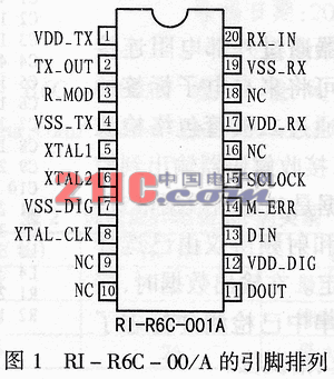
Figure 1 shows (Ri-RRC-001A chip and pin arrangement).
3 Internal structure
The transceiver requires a 5V external power supply. In actual operation, the minimum voltage is 3V, the maximum voltage is 5.5V, and the typical voltage is 5V. The electrical loss depends on the antenna impedance and the configuration of the output network. Because power supply ripple and noise will seriously affect the performance of the entire system, Texas Instruments recommends the use of standard power supplies.
The output transistor inside the RF transceiver is a low-resistance field effect tube, and the power consumption is directly consumed at the TX_OUT pin. It is recommended to use a 5V power supply, preferably driving a 50Ω antenna. Connecting a simple resonant circuit or matching network at the output can reduce harmonic suppression, and driving the output transistor with a gated square wave can achieve 100% modulation. Adjusting the resistance of the output transistor (R2 in a typical circuit) can obtain a modulation degree of 10%. Increasing this resistance increases the modulation degree. The data transformed by the transmitting encoder can be transmitted according to the pre-selected radio frequency protocol. The communication rate should be 5 to 120 kb, and at least one rate must meet the requirements of the selected sensor protocol.
After the receiver is connected to the antenna through an external resistor, the modulated signal from the electronic tag can be demodulated by diode envelope detection. The data output by the receiver decoder to the controller is in a binary data format. The communication rate and RF protocol are selected by the selected mode. determine. When outputting data, the start, stop and error bits have been detected and marked in the received data string. 
The normal clock frequency of the system is 13.56MHz, but the operating frequency range of the oscillator is 4MHz ~ 16MHz.
After the power supply is restarted, the device is in the default configuration. The RI-R6C-001A system has three effective power modes. The main mode is the full load mode, while the no-load mode only appears when the standard oscillator related to the circuit and the standard oscillator in the minimum system operation are stopped. The power-down mode completely shuts down the bias system inside the device. When SCLOCK remains high, the circuit can be woken up at the rising edge of the output pulse at the DIN terminal.
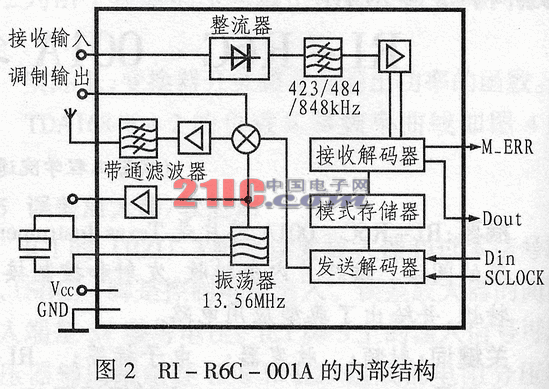
The serial communication interface of the RI-R6C-001A chip usually uses three wires, among which SCLOK is a serial bidirectional clock; DIN is data input and DOUT is data output. Refer to the internal structure diagram of RI-R6C-001A shown in Figure 2.
4 Typical circuit applications
Figure 3 shows the typical application circuit of the RI-R6C-001A. This circuit can drive a 50Ω antenna. When the power supply voltage is 5V, the output RF power is 200mW, and when the power supply voltage is 3V, the output RF power is 80mW. .
image 3
Since the transmitter in the circuit has been working, the size of the heat sink of the integrated circuit should be increased to increase the heat dissipation area. When designing the circuit, you should avoid excessively large distributed capacitance. When the distributed capacitance of the circuit board is too high, you can adjust the value of the capacitor C5 with the crystal to reduce the instability of the clock. The recommended C5 value is 22 pF. Through software processing, the modulation degree of the transceiver can be adjusted within the range of 100% to 10%. The ISO 15693 agreement stipulates that the label allows to perform a modulation degree between 10% and 30% (except 100%), which can be achieved by changing the value of the resistor R2.
5 Conclusion
The RI-R6C-001A integrated circuit is a high-performance, low-cost non-contact induction transceiver chip. It has fast read and write speeds, and can realize multi-target recognition and motion recognition. It can be widely used in logistics management, vehicle anti-theft, and documents. In the fields of anti-counterfeiting, urban taxi management, library management, gun management, etc., with the development of China's electronic label standards, the device will have greater development and application value.
E-mel kepada pembekal ini

Privacy statement: Your privacy is very important to Us. Our company promises not to disclose your personal information to any external company with out your explicit permission.

Fill in more information so that we can get in touch with you faster
Privacy statement: Your privacy is very important to Us. Our company promises not to disclose your personal information to any external company with out your explicit permission.